


On this page
Roughly 480 lumens is available from one 5050 surface-mount package and from one chip-scale package measuring 1.8 by 1.45 millimetres, and the two parts behave nothing alike inside a lamp. The SMD, the COB and the CSP differ in where light leaves the package, how heat leaves it, and how much of the optics job the package has already done before the beam ever reaches a reflector or a lens. Package choice is an optical and thermal decision before it is a brightness decision.
This article compares the three package families as devices. It covers what each one physically is, what its emitting surface does to beam shape, where its heat goes, what its published numbers do and do not mean, and how the choice shows up in assembly cost and reliability. The driver circuit, the thermal design of the complete lamp, the secondary optic, colour binning and lumen maintenance are separate subjects; they are linked where they matter and are not re-explained here.
Quick answer
An SMD package carries a die on a leadframe or a small submount, adds a phosphor layer and usually a lens or a reflecting white body, and is soldered to a board by two pads. A COB mounts many dies on one substrate under a single phosphor layer, so the component presents one large continuous emitting surface instead of a grid of small ones. A CSP builds the package on the die itself, so the finished part is close to die size and adds very little width around the light source.
On cost per lumen the SMD usually wins, because the parts are standardised, reel-packed and run on ordinary surface-mount lines. On luminance, meaning lumens per square millimetre of emitting surface, the CSP wins, and luminance is what a narrow beam needs. The COB wins when a large amount of flux has to come from one component without building a large optical array. The SMD vs COB LED question is therefore usually framed as a two-way choice, and adding the third family is what turns it into a design decision.
| Question | SMD | COB | CSP |
|---|---|---|---|
| What the package adds around the die | Leadframe or submount, white body, phosphor, often a lens | One substrate carrying many dies, one phosphor layer | Almost nothing: the package is built on the die |
| Emitting surface | Small per package, repeated across the board | One large continuous surface | Close to die area, the smallest of the three |
| Dies per component | Usually one | Many | Usually one |
| Power per package at the datasheet condition | 0.18 W to 2.25 W in the parts cited here | 3.1 W class to 84 W class | 3.25 W in the part cited here |
| Where heat leaves the package | Through the leadframe into the board | Laterally through the substrate into the board | Through a die heat sink or direct heat-sink mounting |
| Work left for the secondary optic | Most of it | A large share, because the source is large | The least, which is why it suits tight beams |
| Assembly | Ordinary reflow, high placement count | One placement, one large pad | Reflow with tight pad and stencil control |
| Typical automotive job | Signal, marker, daytime running, arrays | Work and flood light, area light | Headlamp, adaptive beam, focused auxiliary |
The three families are not a ladder. A lamp picks the family that matches its optics, its board and its assembly line, and a vehicle commonly uses more than one.

What a package actually is, and what it is not
An LED package does four jobs. It connects the die to the circuit, it conducts heat from the die into the board, it bounds or shapes the light leaving the die, and it protects the die from moisture, sulfur and mechanical damage. Every feature of a package, whether a white body, a silicone lens, a ceramic substrate or a metal heat sink, exists to do one of those four jobs better or more cheaply than the alternative.
A package is not the die. Two parts in the same package family can carry different dies, and Cree’s own 2835 tables show this directly: one 2835 variant is rated to a maximum of 0.5 W and 0.150 A, while another variant in the same family is rated to 2 W and 0.480 A. The package outline is shared; the silicon and the thermal design behind it are not. Nor is the package the bin, the colour point or the driver, since one 2835 family spans 80 and 90 CRI options and 2200 K to 6500 K, and the bin a lampmaker buys is a purchasing decision made after the package is chosen. That question has its own treatment in white LED colour binning and chromaticity.
What the package does determine, and determines strongly, is the size and shape of the light-emitting surface, the length and width of the thermal path, the number of solder joints per lumen, and the number of components the assembly line has to place. Those four consequences are what the rest of this article is about.
SMD: the leadframe, the white body and the lens
A surface-mount LED is a die sitting on a leadframe or a small ceramic submount, covered by a phosphor layer, enclosed by a white body that reflects sideways light back out of the top, and often topped with a silicone lens. Cree’s J Series 2835 specifications label the products as SMD White Body, which is a description of exactly this construction.
The electrical and thermal connection is made through pads on the underside. Heat produced at the junction travels down through the die attach, into the leadframe, and out through those pads into the board. The white body is not a thermal element; it is an optical one, and its job is to stop light being lost sideways inside the package.
Published numbers for two variants of one 2835 family show how wide the SMD range is inside a single footprint. The lower-rated part runs at a binning current of 0.060 A with a typical forward voltage of 2.91 V, a maximum current of 0.150 A and a maximum power of 0.5 W. The higher-rated part runs at a binning current of 0.065 A with a typical forward voltage of 2.70 V, a maximum current of 0.480 A and a maximum power of 2 W. Cree states 227 lumens per watt typical for that second part at 4000 K, 80 CRI and 65 mA.
The 5050 family goes further. Cree’s J Series 5050 table lists maximum power of 6 W across the family, maximum currents from 0.240 A to 1.000 A, voltage classes of 6, 9, 24 and 30 volts, and typical flux at 4000 K and 70 CRI from 223 to 480 lumens. The whole spread sits under one product name.
The strengths of the SMD follow from that construction. The footprint is standardised enough that second sources exist, the parts arrive on tape for pick-and-place, the assembly is ordinary reflow, a failed emitter can be replaced on a repaired board, and a bar can be built from as many or as few as the design needs. Some SMD parts also include a lens, which shapes the light before it reaches the secondary optic.
The limits follow from the same construction. Flux per package is modest, so a high-output lamp needs many packages, each with its own joints, its own bin and its own place in the assembly sequence. The white body and lens also consume board area that produces no light, which is why an SMD lamp’s emitting surface is a grid of small squares rather than one continuous area.
The 2835, 3030, 3535 and 5050 numbers are footprints, not specifications
The four-digit numbers in LED part names are family labels. They signal a size class and a mounting convention, and that is all they signal. They do not fix the die, the emitting area, the voltage class, the current rating, the power rating or the efficacy.
Cree’s 5050 table makes the point without any interpretation. Inside the family, the published light-emitting surface is listed as either 4.5 mm or 7 mm depending on the part. The voltage class ranges from 6 to 30 volts. The binning current ranges from 0.045 A to 0.400 A. Typical flux ranges from 223 to 480 lumens. Maximum power is 6 W for every part. One label, four different electrical designs and two different emitting areas.
Nichia’s catalogue makes the same point from the other direction. The company files its 757 part under middle power with a 3030 annotation, files its 144 part under super high power with a 5050 annotation, and files its B35 part under super high power and its 19 part under high power, both with a 3535 annotation. The same footprint label therefore appears in more than one power class within one manufacturer’s own range.
There is a further caution. Nichia’s 131 series carries a label that looks like a dimension, but the published package size of the NCSW131H is 1.8 by 1.45 by 0.75 millimetres. The label is a series name, not a measurement, and any comparison that begins by converting a part number into millimetres begins with an assumption the manufacturer never made.
| Label in the part name | What it reliably tells you | What it does not tell you | Evidence from the sources used here |
|---|---|---|---|
| 2835 | A size class and a mounting convention | Die size, maximum power, efficacy, emitting area | One 2835 variant is rated 0.5 W and 0.150 A; another is rated 2 W and 0.480 A |
| 3030 | A size class label used in a catalogue | Which power class the part belongs to | Nichia files its 3030 part under middle power, so the label alone does not establish a power class |
| 3535 | A size class label used in a catalogue | Thermal resistance, lens presence, bin | Nichia files 3535 parts in two different power classes in its own catalogue |
| 5050 | A size class with a family convention | Emitting area, voltage class, current rating | Cree lists 4.5 mm and 7 mm emitting surfaces, 6 to 30 volt classes and 0.045 A to 0.400 A binning currents in one 5050 family |
| 131, 170, 179 | A manufacturer’s own series name | Package dimensions | The 131 series package measures 1.8 by 1.45 by 0.75 millimetres |
The practical consequence is that a specification sheet which says only “2835” or “5050” has told the buyer nothing that can be compared. The comparison has to be made on binning current, test temperature, emitting area, voltage class and maximum power, and those five numbers are what a datasheet exists to provide.
COB: many dies, one substrate, one emitting surface
A chip-on-board package mounts a group of dies directly on a substrate and covers the whole group with one phosphor layer. The result is a single, continuous, usually circular emitting area with no visible gaps between emitters. Lumileds uses the expansion chip-on-board for the family, and Nichia describes its own COB range as ceramic COBs chosen for withstand voltage and durability.
The numbers published for Nichia’s COB range show how far the format scales. In the H6 series, rated at 5000 K with a colour rendering index of at least 90, the range runs from a 3.1 W class part at 176 lumens per watt to an 84 W class part at 173 lumens per watt. In the V5 series, rated at 5000 K and a colour rendering index of at least 80, the range runs from a 3.1 W class part at 181 lumens per watt to an 84 W class part at 170 lumens per watt. The largest part in the published list is an 84 W class device.
Multiplying the two published figures gives an order of magnitude for the top of the range: 84 W at 173 lumens per watt is about 14,500 lumens from one component. That figure is a calculation from the two published numbers, not a datasheet value, and it assumes the part is driven at the power class it is named for.
That single component is the whole argument for COB. One placement, one thermal interface, one optic, one set of solder joints, and a very large amount of light. For a work light or a flood lamp, where the job is to fill an area evenly, a large continuous source is an advantage: there are no dark gaps between emitters to smooth out, and the optic only has to spread light, not collect it from a grid.
The same property is the argument against COB for a narrow beam. A large emitting surface cannot be imaged into a small spot without discarding light, so a COB lamp that claims a long throw is claiming something its source geometry makes expensive. The relationship between source size, beam angle and peak intensity is worked through in reflector cup versus TIR lens, and it applies here as a limit on what any package can be asked to do.
There is a qualification detail that matters for procurement. A COB is a multi-die module, and the automotive qualification system has separate documents for that class of part, including a dedicated stress-test document for optoelectronic multichannel modules. A supplier who says only “AEC qualified” without naming which document is answering a different question from the one being asked.
CSP: the die with its package built on top
A chip-scale package is what its name says. Nichia’s chip-scale family page describes the parts as small LEDs that are as close to chip size as possible, and its 321 series page describes that part as one of the ultimate forms of the idea, with the electrodes on the top of the package rather than beside it. The point of the construction is that almost nothing sits between the die and the outside world.
The thermal arrangement is the distinctive part. Nichia states that the 131 and 121 series include a die heat sink, and that heat dissipation improves further when the part is mounted on a board with a heat dissipation pad. For the 321 series the company describes direct heat-sink mounting, with heat conducted directly to the heat sink. In both cases the first segment of the thermal path, from junction to package, is short by construction.
A published part makes the format concrete. The Nichia NCSW131H product data gives a package measuring 1.8 by 1.45 by 0.75 millimetres, rated at 3.25 W, with a typical forward voltage of 3.25 V and a luminous flux of 475 lumens under the stated test condition of 1000 mA at a junction temperature of 25 degrees Celsius. It is qualified to AEC-Q102, is supplied at 3500 pieces per reel, and has been in production since February 2025.
Two derived numbers are worth stating, with the caveat that both are this article’s arithmetic rather than datasheet values. Dividing 475 lumens by 3.25 W gives about 146 lumens per watt at the stated 25 degrees Celsius junction temperature. Dividing 1000 mA by the 2.61 square millimetres of package footprint gives about 383 milliamps per square millimetre of package area, which is a rough proxy for how hard the part is being driven and not a die current density.
That proxy explains both the appeal and the difficulty of CSP. The appeal is luminance: a very small emitting area carrying a large flux is exactly what a projector-style optic wants, which is why Nichia lists headlamp, adaptive driving beam, daytime running light, turn indicator, rear lamp, car body lighting and head-up display as applications for the family. The difficulty is the board: a small package concentrates heat into a small pad, so the board’s thermal design stops being a detail. Nichia publishes a separate application note on thermal design considerations for printed circuit boards used with its 170 and 131 series, which is a fair indication of where the engineering effort goes.
The three packages side by side, with their test conditions
Published efficacy numbers are only comparable when the conditions behind them are the same, and across these three families the conditions are not the same. The table below sets out what each source actually states, keeps every manufacturer’s numbers in its own column, and adds a calculated efficacy only where the source gives both flux and power at one condition.
| Part and family | Source | Condition stated by the source | Flux or flux class | Efficacy as published | Maximum power | Package note |
|---|---|---|---|---|---|---|
| Cree JB2835 W Class | Cree J Series 2835 | Binning current 0.060 A, typical Vf 2.91 V | Not stated in the row | Not stated in the row | 0.5 W | SMD white body, 80 and 90 CRI, 2200 K to 6500 K |
| Cree JB2835B F Class Pro9 | Cree J Series 2835 | 4000 K, 80 CRI, 65 mA | Not stated in the row | 227 lm/W typical | 2 W | Same 2835 family, four times the power rating |
| Cree JK5050B H Class | Cree J Series 5050 | 4000 K, 70 CRI, 6 V class, 0.180 A | 223 lm typical | 224 lm/W typical | 6 W | Emitting surface listed as 7 mm |
| Cree JR5050C E Class | Cree J Series 5050 | 4000 K, 70 CRI, 6 V class, 0.400 A | 480 lm typical | 213 lm/W typical | 6 W | Emitting surface listed as 7 mm |
| Cree JR5050 P Class | Cree J Series 5050 | 4000 K, 70 CRI, 6 V class, 0.400 A | 442 lm typical | 192 lm/W typical | 6 W | Emitting surface listed as 4.5 mm |
| Nichia NCSW131H | Nichia product data | 1000 mA, junction temperature 25 C | 475 lm | About 146 lm/W, calculated | 3.25 W | CSP, 1.8 by 1.45 by 0.75 mm, AEC-Q102 |
| Nichia COB H6 series, low end | Nichia COB range | 5000 K, Ra at least 90 | 3.1 W class | 176 lm/W | 3.1 W class | Ceramic COB |
| Nichia COB H6 series, high end | Nichia COB range | 5000 K, Ra at least 90 | 84 W class | 173 lm/W | 84 W class | Ceramic COB |
Three observations follow directly from the table, and all three are visible without leaving the published numbers.
Three patterns in that table are worth naming. The highest efficacy figures belong to parts driven gently: the 2835 at 65 mA reaches 227 lumens per watt, the 5050 at 0.180 A reaches 224, and the same 5050 family at 0.400 A reaches 192 to 213, which isolates drive current as the variable because package, colour point and manufacturer are held constant. The CSP figure of about 146 lumens per watt is not a worse part than the 2835; it is a part run at roughly fifteen times the current per package and measured at a junction temperature of 25 degrees Celsius. And the COB figures cluster between 170 and 181 lumens per watt across a range from a 3.1 W class part to an 84 W class part, because the substrate spreads heat across many dies and keeps the current density per die moderate.
Emitting area and why it decides the optics
The emitting area of a package sets what a secondary optic can do with it. A reflector or a lens works by collecting light from a source and redirecting it into a beam, and the source has a finite size. The smaller that size is relative to the optic, the more tightly the optic can concentrate the light, and the higher the peak intensity for a given flux.
This is why the same lumens can produce very different beams, and it is why the emitting area matters more than the package name. Cree’s 5050 family, which publishes its light-emitting surface as either 4.5 mm or 7 mm depending on the part, is a compact demonstration: within one family name there are two source sizes, and the intensity through a shared optic will not be the same.
It is also why CSP suits headlamps. A 1.8 by 1.45 millimetre emitting area lets a small projector or a shallow reflector produce a controlled cut-off, which is the whole problem in a headlamp. Nichia’s application list for the family, which runs from headlamp through adaptive driving beam to daytime running light, is consistent with that reasoning.
SMD sits in the middle. The package is small enough to be useful behind a TIR lens, and a grid of them behind an array of lenses is the standard construction for a light bar. The cost of that approach is that each lens has to be aimed and that the gaps between packages have to be managed optically. Whether a reflector cup or a TIR lens is the better partner for a given package is a separate decision, and the mechanism belongs to the article linked above rather than here.
COB sits at the other end. A large continuous source is easy to spread and hard to concentrate. For a flood beam the source size is not a liability, because the beam is meant to be wide; for a spot beam it is.

Thermal path: where the heat goes in each package
Heat leaves an LED in three stages: from junction to package, from package to board, and from board to ambient. The package family decides the first stage and strongly influences the second. The third stage is the lamp’s business, and it is covered in LED light bar thermal management.
In a CSP the first stage is short by construction. The 131 and 121 series include a die heat sink, and the 321 series is described as mounting directly to a heat sink. There is very little material between the junction and the board pad, which is good for thermal resistance and demanding for the board, because the heat arrives in a small area. Nichia’s separate application note on printed circuit board thermal design for the 170 and 131 series exists precisely because that interface is where the design succeeds or fails.
In an SMD the first stage is longer and wider. Heat crosses the die attach into a leadframe that spreads it over the whole package footprint before it reaches the pads. The thermal resistance of that path is higher than a direct die heat sink, but the heat flux density at the board is lower, which makes the board easier to design.
In a COB the substrate does the spreading. Many dies sit on one ceramic substrate, the heat spreads laterally across it, and the whole component presents one large thermal pad to the board. Total power per component is high, but the area over which it is delivered is also large. Nichia’s choice of ceramic for the family is consistent with that role, and the company emphasises withstand voltage and durability alongside it.
| Package | First thermal segment | Shape of the heat load at the board | What the board design has to solve |
|---|---|---|---|
| CSP | Junction to die heat sink or direct heat-sink mounting | Small area, high flux density | Getting heat out of a small pad without delamination or solder fatigue |
| SMD | Junction through die attach into a leadframe that spreads laterally | Larger area, lower flux density per package | Total heat across many packages, plus pad-to-pad consistency |
| COB | Junction into a shared substrate that spreads laterally across many dies | Large area, high total power | Uniform contact over a large pad, and mechanical flatness |
No thermal resistance values are quoted in this article. Those numbers are published per part, and Nichia maintains a dedicated application note listing thermal resistance values for its 121, 131, 139, 170 and 179 series together with a note on how to calculate junction temperature for the same families. The values in those documents belong to those parts and cannot be transferred to another vendor’s package with a similar name. Where a design depends on the number, the number has to come from the specific part’s own documentation.
Efficacy: comparing lumens per watt without fooling yourself
Efficacy comparisons fail for four reasons, and all four are visible in the table above. The drive current differs, the colour point differs, the colour rendering requirement differs, and the test temperature differs.
Drive current is the largest of the four. Inside Cree’s 5050 family, a part specified at 0.180 A is published at 224 lumens per watt while a part specified at 0.400 A is published at 192 to 213 lumens per watt at the same colour point. The package is the same size class, the manufacturer is the same, the colour temperature and rendering index are the same, and only the current changed. A buyer who compares a 224 figure against a 192 figure and concludes that one supplier is better has compared two drive conditions, not two companies.
Colour point and rendering matter in the same way. Nichia’s own COB catalogue shows the effect: the series rated at a colour rendering index of at least 90 runs from 171 to 179 lumens per watt, while the series rated at 80 runs from 170 to 181. The higher-index part is doing more spectral work, and the two should not be ranked as if they were the same product.
Test temperature is the one that is easiest to miss. The Nichia CSP figure is quoted at a junction temperature of 25 degrees Celsius. That is a measurement condition, not an operating condition. A lamp in a housing on a summer night does not run its junctions at 25 degrees Celsius, and how much flux is lost at real operating temperature is a property of the specific part, published in its own documentation and in its lumen maintenance data rather than in a headline efficacy figure.
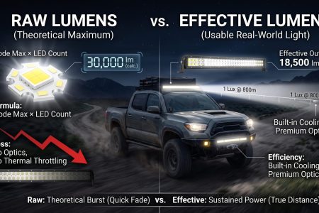
The fourth trap is arithmetic across a whole lamp. A package efficacy is not a lamp efficacy. The driver loses power, the optic loses light, the housing absorbs some, and the thermal design decides how much of the published flux survives. The difference between the two is the subject of raw lumens versus effective lumens, and it is larger than most package-level differences discussed here.
Current density: the number that explains the heat
Current density is the variable that ties the three families together. It is not published as a single number, but it can be read from the test conditions, and it explains why the same flux can arrive with very different thermal consequences.
The 2835 part in Cree’s table is specified at 65 mA and reaches 227 lumens per watt at 4000 K and 80 CRI, with a typical forward voltage of 2.70 V. At that condition the part consumes about 0.18 W and produces roughly 40 lumens. Both figures are calculations from the published numbers, and they set up the comparison that follows.
To reach the 480 lumens that one Cree 5050 part produces at 0.400 A, a designer using those 2835 parts needs about twelve of them. Twelve packages at 0.065 A each draw 0.78 A in total, consume about 2.11 W, and produce about 477 lumens. One 5050 part at 0.400 A and 5.63 V consumes about 2.25 W and produces 480 lumens. One Nichia CSP at 1.000 A and 3.25 V consumes 3.25 W and produces 475 lumens.
| Route to about 480 lumens | Packages needed | Current per package | Total current | Total power | Package count consequence |
|---|---|---|---|---|---|
| Cree 2835 F Class Pro9 at 65 mA | 12 | 0.065 A | About 0.78 A | About 2.11 W | Twelve placements, twelve joints sets, twelve bins to match |
| Cree JR5050C E Class at 0.400 A | 1 | 0.400 A | 0.400 A | About 2.25 W | One placement, one optic interface, one thermal pad |
| Nichia NCSW131H at 1.000 A | 1 | 1.000 A | 1.000 A | 3.25 W | One tiny placement, one small high-flux pad, tight stencil control |
The table contains the whole argument in one place. The three routes land within about 12 percent of each other on flux and within about 50 percent on power, and they differ by a factor of twelve on component count and by a factor of 2.5 on current per package. Twelve packages mean twelve placements to inspect, twelve joint sets, twelve parts to bin-match and twelve thermal pads; one package means one of each, but all the heat arrives in one place, the optic has to work with one source geometry, and one component failure takes out the whole output.

The current per package also sets the conductor and the driver. A single CSP at 1.000 A is a different load from twelve 2835 parts at 0.065 A each, even though the total flux is the same. Series and parallel arrangements, current sharing between parallel strings and the effect of one string opening are all consequences of the package count, and Nichia addresses part of that territory in an application note on the parallel connection of gallium nitride LEDs.
Reliability: joints, phosphor and die attach
A package decides which failure modes a lamp can have. The mechanisms are the same physics in all three families, but the number of places each mechanism can act is not.
The joint count is the most obvious difference. Building about 480 lumens from 2835 parts at 65 mA takes twelve packages, so it takes twelve sets of solder joints, twelve placements and twelve parts that have to be bin-matched to each other. The same flux from one 5050 or one CSP takes one set. Fewer joints is fewer opportunities for a crack, but the joints that remain carry far more current each, so the consequence of one bad joint is larger.
Solder cracking in automotive LEDs is a documented enough concern that Nichia publishes an application note on solder crack considerations for LEDs used in automotive applications. Sulfur corrosion is documented in the same way, with a note on how it occurs and how to avoid it. Neither note is specific to one package family, and both are worth reading before assuming that a package is protected because it is small.
The phosphor is the second place where the families differ. White light from a blue die is produced by phosphor conversion, one of the three routes to white light that the U.S. Department of Energy describes. In an SMD the phosphor sits inside a package that also contains a white body and often a lens; in a COB one layer covers many dies; in a CSP the layer is close to the die with very little material above it. How much blue light and heat that layer sees depends on the construction, and how fast it changes is a matter for the part’s own lumen maintenance data rather than for a general rule.
Mechanical stress is the third. A CSP has almost no compliant material between the die and the board, which is good for heat and unforgiving for board flex; the automotive qualification system addresses that specifically with a board flex test as part of the Q102 family. A COB spreads a large rigid substrate over a large pad, so flatness and coplanarity matter. An SMD’s leadframe absorbs some of the mismatch between board and package.
| Package | Failure mode worth designing against | Why the package shape matters | Where to look for evidence |
|---|---|---|---|
| CSP | Solder fatigue at a small, heavily loaded joint | Tiny pad carries the whole current and heat flux | Vendor notes on solder cracking; board flex test in the Q102 family |
| COB | Substrate or interface cracking under thermal cycling | Large rigid area, high total power, one pad | Multichip module qualification documents; the part’s own cycling data |
| SMD | Joint cracking and encapsulant or lens degradation over many parts | Many small joints, polymer materials in the light path | Vendor reliability data; the part’s lumen maintenance report |
Cree publishes reported lifetime figures for its 5050 family of more than 109,000 hours to L90 and Q90 for two of its series. Those are reported figures for those parts under the conditions of the underlying test, not a promise about a finished lamp, and they illustrate the right way to use such a number: as a property of a specific part, quoted with its threshold and its basis, not as a property of a package shape.
What AEC-Q102 qualifies, and what it does not
AEC-Q102 is titled as a failure-mechanism-based stress test qualification for discrete optoelectronic semiconductors in automotive applications. It is part of a family of documents maintained by the Automotive Electronics Council, and the family statement is explicit: components meeting these specifications are suitable for use in the harsh automotive environment without additional component-level qualification testing.
The sub-documents matter when a supplier claims compliance for a multi-die part. The Q102 family includes a dew test, a board flex test, and a separate document for optoelectronic multichannel modules. Multi-chip modules more generally have their own qualification document, AEC-Q104, and board-level reliability has yet another, AEC-Q007, which includes a board-level reliability temperature cycling test method.
| Document | What it covers | Why it matters when comparing packages |
|---|---|---|
| AEC-Q102 | Stress test qualification for discrete optoelectronic semiconductors | The base qualification for a single-die CSP or SMD |
| AEC-Q102-001 | Dew test | Moisture behaviour at the package level |
| AEC-Q102-002 | Board flex test | Mechanical strain through the board, which a CSP passes through a very small joint |
| AEC-Q102-003 | Optoelectronic multichannel modules | The relevant document when one component contains many dies |
| AEC-Q104 | Multichip modules | The general module qualification, relevant to COB |
| AEC-Q007 | Board-level reliability, including temperature cycling | Where the board, not the component, is the thing being qualified |
What AEC-Q102 does not do is equally important. It is not a lamp approval, it does not establish compliance with any vehicle lighting regulation, it does not give a lifetime in hours, and it does not qualify the board the part is soldered to. A datasheet line that says AEC-Q102 qualified tells a buyer that one specific component passed one specific set of component-level stress tests. It says nothing about the housing, the optic, the driver or the assembly.
Cost: components, joints and assembly steps
No public price list exists for these parts, so any quoted package price is an estimate from an unknown date. What can be reasoned about is structure.
An SMD route spends money on components and placements: twelve 2835 parts cost twelve component prices and twelve placements, and the board needs twelve footprints with their pads, silkscreen and inspection points. Against that, the parts are the cheapest per lumen in volume, the assembly is standard, and the supply base is wide.
A CSP route spends money on precision. One part replaces twelve, which cuts placement count, reel count and joint count, but the pad geometry, the stencil and the reflow profile have tighter windows, and the board has to remove a large amount of heat from a small area. A COB route spends money on the interface: one component replaces an array, one optic replaces an array of optics, and what it demands in return is a large, flat, well-coupled thermal interface held under load for years.
| Cost and effort driver | SMD | COB | CSP |
|---|---|---|---|
| Components per 480 lumens | About 12 in the worked example | 1 | 1 |
| Placements per 480 lumens | About 12 | 1 | 1 |
| Solder joint sets | About 12 | 1 | 1 |
| Board area for the light source | Large, and partly lost to white body and lens | One large pad | Very small pad |
| Process window | Wide, standard reflow | Wide for placement, tight for thermal interface | Tight for stencil, placement and reflow |
| Board thermal design effort | Moderate, spread over many pads | Moderate, one large area | High, small area with high flux |
| Optics count | One per package, or one array element per package | One | One |
| Where the cost moves as volume rises | Component price | Substrate and assembly | Component price and yield |
The direction of each column is the useful part: SMD trades process simplicity for component count, COB trades component count for interface quality, and CSP trades interface quality for process precision.
Why automotive lamps use all three
A vehicle does not pick one package family. It picks a different one for each lighting job, because each job asks a different question of the source.
A headlamp needs a controlled cut-off and a high peak intensity from a small aperture, so it wants the smallest emitting area that can carry the required flux. Nichia’s application list for its chip-scale family, which runs from headlamp through adaptive driving beam and daytime running light to turn indicator, rear lamp, car body lighting and head-up display, is a catalogue-level statement of that fit. The other jobs pull in different directions, and the pattern is consistent enough to tabulate.
| Lighting job | What the optic needs from the source | Package family that fits naturally | Why the other two fit less well |
|---|---|---|---|
| Headlamp, adaptive beam | Small emitting area, high luminance, precise positioning | CSP, high-power small-area packages | An SMD array multiplies alignment work; a COB source is too large to image |
| Daytime running light, marker | Shape and uniformity, low power, low cost | SMD arrays | CSP adds cost without a beam benefit; COB is more flux than the job needs |
| Rear lamp, signal | Broad even surface, shallow depth | SMD arrays, some COB | A small CSP gives a point source that must be spread |
| Work light, flood | High total flux, wide even field | COB, SMD arrays | CSP concentrates heat and flux where the job wants spread |
| Focused auxiliary spot | High candela from a compact housing | CSP, small high-power packages | COB cannot be concentrated without large losses |
Common misreadings of package names
Most SMD vs COB LED arguments compare package names and stop there. The five claims below account for most of the confusion, and each one can be checked against numbers already quoted in this article.
| Claim | Why it fails | What to check instead |
|---|---|---|
| More LEDs means a brighter lamp | Emitter count is a design choice, not an output figure | Flux at a stated current and temperature, and the total input power |
| COB is the better technology | It optimises flux per component and source uniformity, not luminance | The emitting area and the beam the optic has to make |
| Smaller packages are more advanced | Smaller packages are harder to cool and to assemble | Current per package, pad area and the board thermal design |
| SMD means low quality | Package shape does not set bin, die quality or lifetime | The part’s own bin, qualification and maintenance data |
| 5050 means 5 by 5 millimetres | Manufacturers publish different emitting areas inside one family | The published emitting area, not the family name |
What to read in a datasheet before comparing
A datasheet that supports a real comparison contains eight lines, and a listing that omits them cannot be compared with anything.
| Datasheet line | What it establishes | What it hides if read alone |
|---|---|---|
| Binning current | The current at which the flux and colour were measured | How the part behaves at the current the lamp will use |
| Test temperature | The junction temperature of the measurement | The flux at real operating temperature |
| Maximum current and power | The design envelope | How much of the envelope is usable in a sealed housing |
| Emitting area | What the optic has to work with | The luminance, unless flux is also known |
| Voltage class | The driver requirement | Efficacy differences between voltage classes |
| Colour point and rendering index | The colour the part was binned to | Colour shift over temperature and life |
| Qualification document | Which stress tests the component passed | Anything about the board, the housing or the lamp |
| Reported lifetime | The threshold and basis of a maintenance claim | Whether the same conditions apply in the application |
Where the package stops mattering, and when to ask an engineer
Package choice sets the ceiling on a lamp, not the result. Three things below the package decide whether that ceiling is reached.
The driver decides how hard the part is actually run and how stable the current is. The thermal design decides what junction temperature the part reaches, and therefore how much of its published flux survives. The optic decides how much of the light that leaves the package arrives where the user needs it. A well-chosen CSP in a poor housing is a worse lamp than a modest SMD array in a good one.
There are also cases where the package question is the wrong question entirely. If the lamp is a road-legal headlamp, the governing constraint is the approval, not the package; if it replaces a regulated signal lamp, the photometric requirement decides the design. Any SMD vs COB LED comparison also depends on a housing that can actually remove the heat, so a sealed housing with no thermal path has to be solved before the comparison means anything.
Ask an engineer rather than a listing when the design is close to the maximum current of the chosen part, when the housing has no thermal path to outside air, when the lamp must meet a photometric or approval requirement, when several packages will be wired in parallel, or when the intended operating temperature is unknown.
A comparison method you can run on two lamps
Two lamps can be compared without a photometric laboratory if the comparison is recorded the same way on both. The six records below are enough to separate package performance from everything around it. Most product pages stop short of them: a 40 inch light bar is listed by length and wattage, a heavy-duty work light by wattage and beam, and the LED light bars category groups products by form factor rather than by package.
| Record | How to take it | Why it changes the conclusion |
|---|---|---|
| Emitter count | Count visible packages | Separates component count from output |
| Emitting area of one package | Measure with the optic removed, or read the part number | Sets what the optic can do |
| Input current and voltage | Measure at a fixed supply voltage | Converts a wattage claim into a real load |
| Emitter part number | Read the marking, or ask the supplier | Makes the comparison specific instead of generic |
| Optic type and element count | Visual inspection | Separates package performance from optic performance |
| Housing volume and sealing | Measure and inspect | Explains thermal behaviour that the package cannot |
The result of that record is usually that two lamps with similar claimed output differ mainly in emitter count, optic count and housing volume, and that the package family is the smallest of the differences. That is not an argument that the package does not matter. It is an argument that the package is one variable among four, and that a comparison which fixes the other three is the only one that isolates it.
Frequently asked questions
Is the SMD vs COB LED comparison still the right question?
It is the right question only if CSP is added as a third option. The two-way version of the SMD vs COB LED comparison dates from a period when chip-scale parts were not common in vehicle lamps. Today a lamp designer chooses among three source geometries, and the choice is driven by the emitting area the optic needs.
What does COB stand for?
COB stands for chip-on-board. The name describes the construction: dies are mounted directly on a substrate and covered by one phosphor layer, so the component presents a single continuous emitting surface rather than a row of separate packages.
Does more LEDs mean a brighter light bar?
No. In the worked example in this article, twelve small packages and one larger package both produce about 480 lumens. Emitter count affects the assembly, the joint count and the optical layout, and it does not by itself determine output. The relevant figures are flux at a stated current and temperature, and total input power.
Is a 5050 LED 5 millimetres by 5 millimetres?
Do not assume so. Cree publishes emitting surfaces of 4.5 millimetres and 7 millimetres inside its 5050 family, and its 5050 parts are offered in 6, 9, 24 and 30 volt classes with maximum powers of 6 W. The number in the name is a family label, and the dimensions have to come from the drawing.
Why do automotive headlamps use CSP?
Because a headlamp needs high luminance from a small aperture. A chip-scale package puts a large flux into an emitting area close to die size, which lets a compact projector or reflector produce a controlled cut-off. Nichia lists headlamp, adaptive driving beam and daytime running light among the applications for its chip-scale family.
Can a COB be replaced by several SMD LEDs?
Sometimes, and the trade is predictable. Replacing one COB with a row of SMD parts multiplies the placement and joint count and changes the source from continuous to a grid, which changes what the optic has to smooth out. It also spreads the heat over more pads, which can be easier on the board.
What is the difference between a 2835 and a 3030?
Both are family labels for a size class, and neither fixes performance. Cree’s 2835 family alone contains a part rated 0.5 W and 0.150 A and a part rated 2 W and 0.480 A. The difference that matters between any two parts is in the binning current, the test temperature, the emitting area and the maximum ratings.
Do package types change the colour of the light?
Not directly. Colour comes from the die and the phosphor, and it is controlled by binning. Package construction does affect how much blue light and heat the phosphor sees, and therefore how colour behaves over temperature and life, but a package name does not predict a colour point.
What does AEC-Q102 on a datasheet prove?
It proves that one component passed a defined set of component-level stress tests for discrete optoelectronic semiconductors in automotive applications. It does not prove that a lamp built from that component meets any lighting regulation, and it does not cover the board, the housing, the optic or the driver.
Editorial note
Written by SAEC Lighting Engineering Team, Foshan. This article compares package constructions only; it does not claim that any specific SAEC product uses a particular package, and it makes no vehicle fitment claim. Where a manufacturer publishes a value, the value is attributed to that manufacturer and kept separate from other manufacturers’ values.
Last updated: 2026-10-20
Sources
- Nichia, Chip Scale Packages (automotive): https://led-ld.nichia.co.jp/en/product/automotive_csp.html
- Nichia, 321 Series (automotive multi-chip CSP): https://led-ld.nichia.co.jp/en/product/automotive_321.html
- Nichia, NCSW131H product data: https://led-ld.nichia.co.jp/en/product/led_product_data.html?type=NCSW131H&kbn=0
- Nichia, COB lighting range: https://led-ld.nichia.co.jp/en/product/lighting_cob.html
- Cree LED, J Series 2835 LEDs: https://www.cree-led.com/products/leds/j-series/2835/
- Cree LED, J Series 5050 LEDs: https://www.cree-led.com/products/leds/j-series/5050/
- U.S. Department of Energy, LED Basics: https://www.energy.gov/cmei/ssl/led-basics
- Automotive Electronics Council, AEC documents (AEC-Q102, Q104, Q005, Q007): http://www.aecouncil.com/AECDocuments.html
- Lumileds, Understanding CoB LEDs (page returned HTTP 200; only the page header and navigation were readable in this environment): https://lumileds.com/technology/led-technology/understanding-cob-leds/
 by


